


By 2025, Intel is aiming to increase its most advanced chip packaging services’ capacity fourfold, driven by the establishment of a new facility in Malaysia.
The goal is to reclaim its global leadership in semiconductor manufacturing, with a particular focus on its cutting-edge Foveros technology, involving advanced 3D chip packaging.
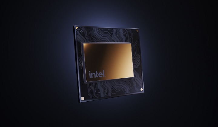
3D chip packaging, also known as 3D packaging or 3D integration, is an advanced semiconductor packaging technology that involves vertically stacking multiple integrated circuits (ICs) or chips on top of each other within a single package.
This initiative includes the construction of a factory in Penang and an additional chip assembly and testing facility in Kulim, Kedah as part of a USD7 billion (RM32.4 billion) expansion in Southeast Asia, according to Nikkei Asia.
Intel’s Penang factory marks a significant milestone as it will be the company’s first overseas facility for advanced 3D chip packaging. The plan is for Malaysia to eventually become Intel’s primary production hub for 3D chip packaging.
Although the exact commencement date for mass production at the Penang facility remains unspecified, it signifies Intel’s strategic commitment to pushing the boundaries of chip packaging technology.
In contrast to the past perception of chip packaging as less critical and less intricate than chip manufacturing, it has now emerged as a pivotal domain in the quest to create more potent chips.
Traditional methods of cramming more transistors into smaller spaces have become progressively challenging. The surge in generative AI advancements this year has further heightened interest in advanced chip packaging.
Mark Li, an experienced semiconductor analyst from Sanford C. Bernstein, has identified the burgeoning interest in advanced chip packaging, attributing it mainly to the demand for handling large artificial intelligence (AI) models in chip design.
Industries are increasingly eager to invest in AI computing, necessitating expanded capacity in advanced packaging. However, for sustained enthusiasm, the proliferation of AI applications remains crucial.
Intel’s pivotal 3D chip packaging technology currently originates primarily from its facilities in Oregon, USA, with a significant production base in New Mexico. The company’s ambitious strategy involves investing over USD10 billion (RM46.4 billion) in New Mexico and Malaysia combined over the next decade to bolster this field.
Malaysia is already a vital hub for Intel’s chip packaging, assembly, and testing operations, with 15,000 employees in the country, including a substantial workforce of 6,000 at its chip design centre. This move positions Malaysia as a linchpin in Intel’s global chip innovation ecosystem.